
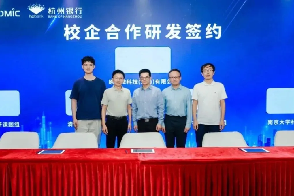
Shanghai-based Yuanjiwei has set up what it claims to be the world’s first pilot production line for 2D semiconductors, reports the South China Morning Post.
Yuanjiwei has released version 0.1 of its PDK for its 500nm 8-inch line and has launched foundry tape-out services.
Yuanjiwei’s chairman, Bao Wenzhong, said the company aims to establish a manufacturing process comparable to a 90nm silicon node by the end of 2026, followed by a fully domestic process equivalent to 5nm chips by 2029 without the use of EUV litho.
Yuanjiwei intends to use heterogeneous packaging to combine 2D and 3D chips.
Many universities and national labs routinely fabricate 2D semiconductors such as MoS₂ or WS₂ transistors, from basic exfoliated flakes to wafer-scale CVD-grown films.
Europe’s 2D Pilot Line project is running prototype services for graphene and similar materials on 200mm wafers
Imec, TSMC and ASML demonstrated a 300mm 2D process last month.